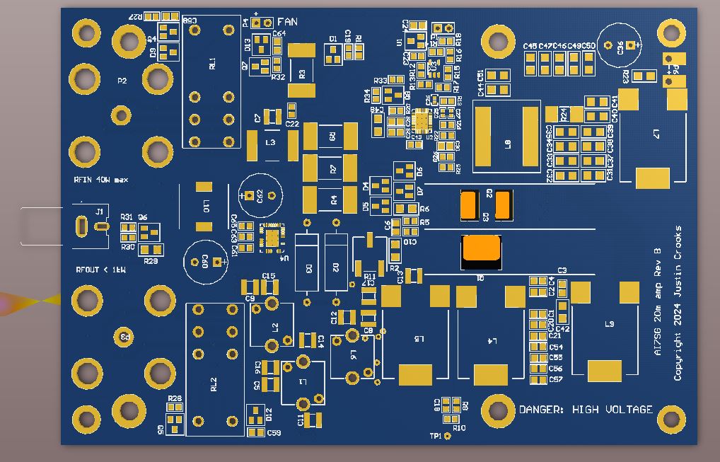
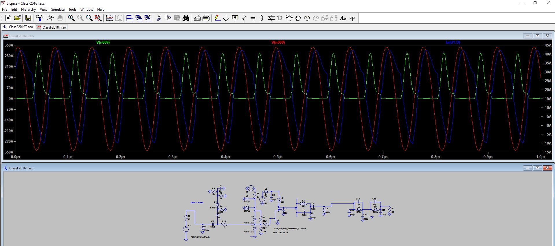
The idea is to design a clean switch-mode power supply that can envelope-track (class H) a SSB or digital narrow-band signal, and use it to drive a Class F ultra-low-loss amplifier with some extra harmonic filtering. Simulations look pretty good, except for how sensitive it is to reactive loads. Targeting 20 meters, 1 kW, >85% efficient for my first design.
Looking at
https://gansystems.com/gan-transistors/gs66516t/
for the RF FET, cooled with a heat pipe and a small CPU fan at half power.
The power supply is a special blend of circuitry built around this:
https://www.analog.com/en/products/ltc7891.html
(The power supply FETs will be cooled with heat pipes as well.
Update 1:
Thanks to a winter storm giving me an extra day off, rev B is ready to order (Rev A was a failure because the FETs I selected were tiny BGAs beyond my ability to solder. Rev B uses equally modern FETs but in a friendlier package.

Simulations are complete. Power supply can ramp up or down over a volt per microsecond, and overall 90% efficiency is predicted. We’ll see! I was a little worried about coupling between L4 and L5 but the only effect when simulated (spice directive K1 L4 L5 0.2 or -0.2) was a small change in gain (which I can easily adjust elsewhere). Designed to fit in a 6″ x 4″ x 5″ enclosure with about 100 watts of active cooling (fills the remaining volume of the enclosure almost perfectly).
I left a clearance for heat pipes over the GaN FETs (both the power supply FETs and the RF amp FET). Those will go to a CPU cooler with a 92mm fan.
Update 2:
Boards and parts are ordered, including the Type N to UHF adapters. 2 oz copper was a bit more expensive, but even with air flow there is just too much trace heating with 1 oz copper!
PCB:
https://www.pcbway.com/ (click from here to get $5 off your 1st order and I get a few bucks off my next order)
Parts:

Leave a Reply